Taking advantage of a short break from studying, I started a project that I started almost a year ago.
This is a headphone amp, I wanted to finally connect to my computer.
almost always listening to the audio in the headphones, I immediately felt the limits of my sound card, both in terms of power output of that band. Low frequencies, in particular, were reproduced with difficulty, and indeed it must be said that the final stage of my "Creative Sound Blaster Live! OEMs" was not exactly designed to drive headphones from 40 ohms (which are mine) , and it was inevitable that such a low impedance strongly influence the dynamic qualities of the card.
I am not aware of the value of output impedance of the board, but it is likely that this is high output impedance.
The choice of the final.
I analyzed a number, because I could use the integrated end-type LM386 or TDA2822M in my possession, I could make a simple buffer BJT, and I even considered a tube glides by new electronics.
Given the cost of that alternative (out of my "budget"), I headed to another kit of the same journal, signed LX1144 (available in the magazine No. 167-168).
This is a final 1 + 1W RMS input FET and MOSFET final, a very elegant solution. The characteristics of "plate" are very attractive, and one can easily obtain a gain of 30 dB.
construction. Kit or spacers?
After I informed, and have gathered opinions uniformly favorable to the kit in question, I decided that I would have built.
However, as I was going to change it, would not make sense to order the complete kit, already had all the components, and my changes would upset the PCB, with unpredictable outcomes. The printed circuit board provided in the kit is in fact equipped with a ground plane, which provides excellent immunity to disturbances, but restricts the possibilities of change. I then collected
all the necessary components, and armed with the proverbial breadboard, I replicated the circuit as it was proposed in the magazine.
Although some details changed immediately went, I also tried this configuration "base" and the result proved to expectations.
A sound clearly different from the "tired" that I used to listen to, the headphones were now being driven by a decision even in the deeper bass while maintaining a more than ample bandwidth (the data indicate a band of 20 to 22,000 Hz, + / - 1 dB!).
While not using a print screen to the ground plane, I have picked up disturbances, except maybe the signal from the phone close by and the use of a matrix board also has its limits!
limits and changes
preplessità My only at this point concerned the weak points "known" in this kit.
First, the endings are made with a pair of complementary MOSFET signed IRFD.1Z3 IRFD.9110 and in HD-1 package, much like a four-pin DIP. New Electronics designers have brilliantly solved the problem of the plinth using a 8-pin DIP socket, which accommodate the P-MOS and N-MOS of each final. This solution, although avoids direct soldering of the FET, it has some limitations. First, it becomes difficult to establish
qualsiati type of heat sink, less than "paste" directly to the finals, also, given the nature of "snap" of the hoof, there is the possibility that the transistor over time become detached from their place, with Results imagine.
Then, even wanting to use a heat sink attached externally to the mold, it collides with the filter capacitors, and with the same problem of 'instability' of the MOSFET on the hoof. It is not appropriate to apply any pressure to the whole "Mosfet + socket," not to bend any pins. In short, you have to work with the MOSFET not dissipated, and, with the currents involved, these components tend to heat up considerably.
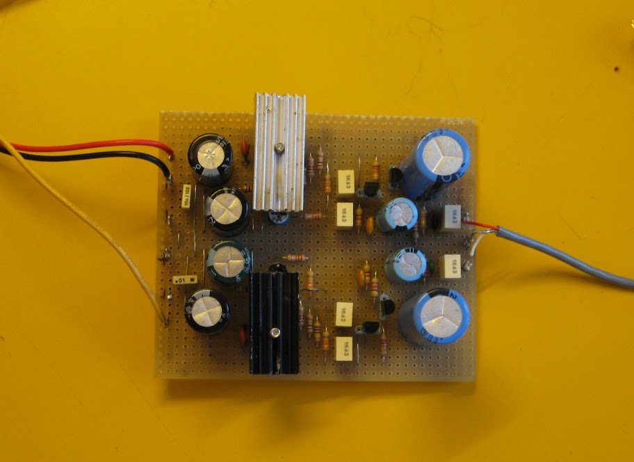
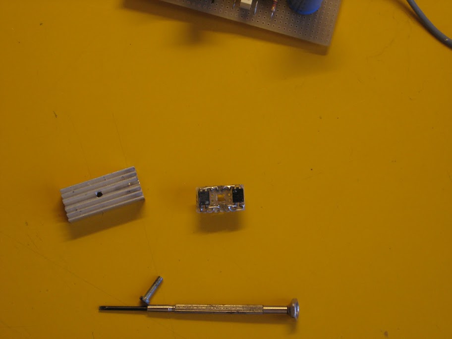
I then placed the MOSFET in a slightly different way, by welding on a support floor, and providing a heat sink. The images easily explained as I did.
The amp is still at the prototype stage, heat sinks are still too close to the capacitors, but with a few more I'll take it arises to change all'assetto final. Here are the results so far:
amplifier without the output transistors. Hooves are visible: Used
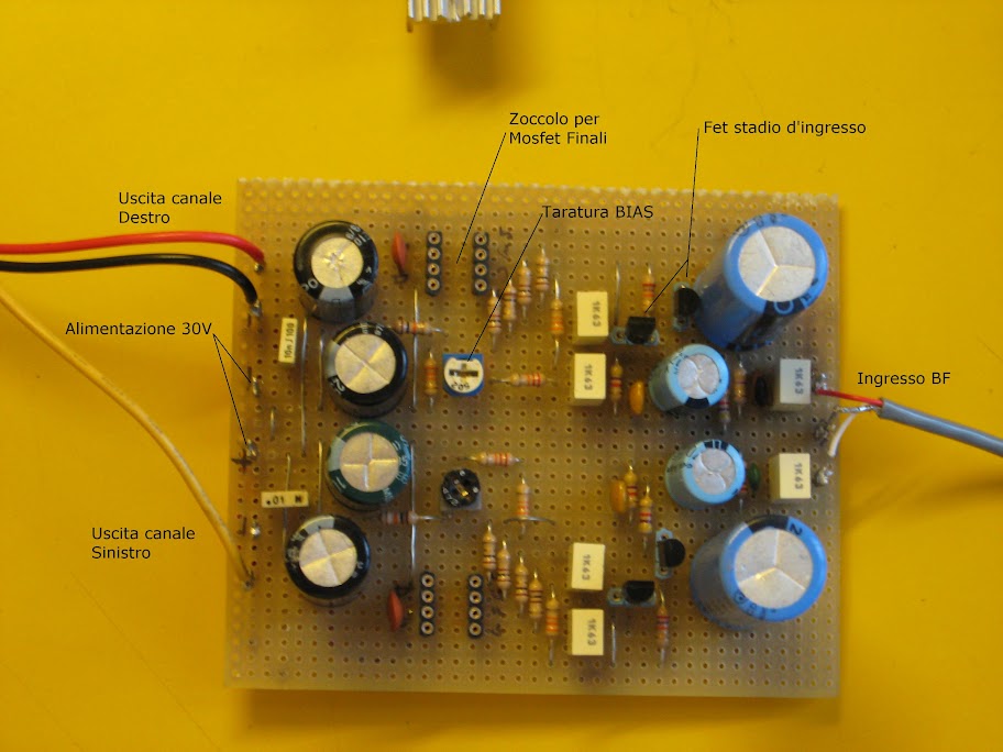
The amplifier in the final in their place:
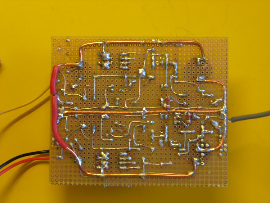
The back of the end. You can see the tracks of large mass (middle), and the two runs for the 30V (which extend to the sides). I made these tracks with copper more often in order to ensure maximum readiness in the current peaks.
An overview of the technique used to mount the transistors on a removable medium and strong. Magnifying the image is easily seen the "trick".

All images can be viewed at full resolution on PICASA .